| 是否进口:否 | 品牌:瀚吉 | 型号:3535 |
| 材质:氮化铝基板 | 外形尺寸:109mm*54mm | 导热系数:170~200W/m .K |
| 热膨胀系数:0.0000043/℃ | 反射率:0.08 | 最大承受光源功率:18w |
| 功能区镀层厚度:65微米 | 防流化处理方式:沉金 | 第一镀层A面:钛 厚度:0.1μm |
| 第二镀层A面:铜 厚度:65±10μm | 第三镀层A面:银 厚度:0.2-0.5μm |
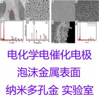
陶瓷基板,陶瓷线路板,氮化铝基板,氧化铝基板加工,线距线宽精度可以达到50微米,中山大学电子封装电化学实验室,加工工艺源于航空科技。
面向微电子公司,采用DPC技术加工陶瓷电路。解决客户陶瓷电路量产订单的加需求。
面向科研院校提供陶瓷电路加工所需化学品。为研究者提供磁控溅射、菲林和电镀加工服务。
以下是3535标准版的介绍,及生产线样片实拍照片:
氧化铝纯度96%,材料板厚0.5mm,镀铜厚度65±15μm,可选双面白色或者绿色阻焊油墨,沉银0.2-0.4μm。
A面镀层情况
镀层层数:***层 材料种类:钛 厚度:0.1μm
镀层层数:***层 材料种类:铜 厚度:65±10μm
镀层层数:第三层 材料种类:银 厚度:0.2-0.5μm
B面镀层情况
镀层层数:***层 材料种类:钛 厚度:0.1μm
镀层层数:***层 材料种类:铜 厚度:65±10μm
镀层层数:第三层 材料种类:银 厚度:0.2-0.5μm
阻焊油墨:可选白色,绿色
A面阻焊油墨厚度:10-13μm
B面阻焊油墨厚度:10-20μm
通孔镀铜,孔径53μm 100μm 53μm
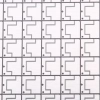
有两种版,一种是正方形,一种是矩形,详情见下图。
Ceramic substrates, ceramic circuit boards, Aluminium Nitride substrates, Aluminium Oxide substrates processing, line width and spacing can reach 50μm.
Sun Yat-sen University Electronic Packaging Electrochemistry Lab, our processing techniques come from space technology.
To microelectronics companies, we adopt DPC technology to process ceramic circuits, meeting their demands for mass production of the ceramic circuits. To scientific research institutions, we provide the required chemicals for ceramic circuits processing. To researchers, we provide the services of magnetron sputtering, film and electroplating processing.
The following is a brief introduction to 3535 standard edition, with sample pictures:
Alumina purity is 96%, material plate thickness is 0.5mm, copper plating thickness is 65±15μm.
The color of solder-resist ink is optional, you can choose double-sided white or green. Immersion silver thickness is 0.2-0.4μm.
Plating layers on Side A
The first layer: material: Ti; Thickness: 0.1μm;
The second layer: material: Cu; Thickness: 65±10μm
The third layer: material: Ag; Thickness: 0.2-0.5μm
Plating layers on Side B
The first layer: material: Ti; Thickness: 0.1μm;
The second layer: material: Cu; Thickness: 65±10μm
The third layer: material: Ag; Thickness: 0.2-0.5μm
Solder-resist ink: white or green
Thickness of solder-resist ink on side A: 10-13μm
Thickness of solder-resist ink on side B: 10-20μm
Hole cut copper plating, apertures are 53μm, 100μm, 53μm
There are two types of 3535 ceramic substrates, one is square, the other rectangle.
实拍样片图片: